6. Copper and tin plating
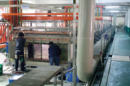
Electro-plating would be an obvious choice to make the vias conductive, except for one minor problem: only already-conducting surfaces can be electro-plated. To get around this, the board is immersed in various chemicals that coat its entire surface with a thin layer of copper. It's a slow method and very expensive, but it provides just enough conducting metal to electro-plate over the top.
Electro-plating the entire board would be wasteful because most of the copper would subsequently be etched away to produce the pads and tracks on the outer layers of the PCB. Instead a photo-resist is applied, exposed to UV light through an artwork and developed as when fabricating the copperclad laminate – but with one important alteration.

Here, a different type of artwork is used so that the photo-resist remains in those areas that don't correspond to the pads and tracks of the finished board. Now the electro-plating will only increase the thickness of the copper on the areas without the insulating photo-resist.
The board is finally electroplated with tin, which, once again, only adheres to those areas of the board that will form the pads and tracks. The tin serves three purposes: it prevents the copper tarnishing; it provides a surface that can be soldered to more easily than copper; and it acts as a resist (after first removing the remaining photo-resist) in the next process – etching away the unwanted copper.
We now have a PCB with copper pads and tracks on the outer two surfaces, tracks on four internal layers, and vias making the necessary connections between the various layers.
To complete the bare PCB, a solder mask and component identification are applied via silkscreen printing. The solder mask covers all of the board where solder shouldn't adhere when the components are fixed in place. This prevents unwanted bridges between tracks that could occur during wave soldering in step 9.
Get daily insight, inspiration and deals in your inbox
Sign up for breaking news, reviews, opinion, top tech deals, and more.
The component identification provides a visible labelling of each of the components with their serial numbers. This is useful in manual inspection or board maintenance.
7. Routing, testing and QA
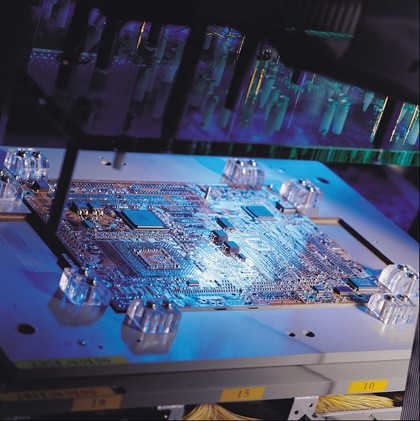
Steps 2 to 7 involved the processing of a panel – a sheet of material comprising several motherboard PCBs. Now the individual boards are separated using a numerically controlled router, which is also used to create any non-plated larger holes and slots that are needed.
The board is then given a going over by a 'bed-of-nails' tester, an automated process that probes both sides of the board to ensure that electrical pathways exist where they are supposed to and that there are no shorts.
Finally, before leaving the PCB fabrication facility, the motherboard is given a QA inspection to ensure it meets its specification in terms of the overall board size, mounting hole tolerances and so on.
8. Surface mounting
The first components to be soldered onto the bare PCB are the surface mountings. Solder paste – a mixture of solder powder and flux – is printed onto those pads on the top surface of the board where the contacts of the surface-mounting components (SMCs) will be soldered. The SMCs are placed on the board using a pick-and-place machine.

The tackiness of the solder paste holds the components in place, but they're not fixed securely and there isn't a proper electrical connection.
The next stage is reflux soldering. The PCB is placed in a reflux oven and heated to over 200C. The solder in the paste melts and then solidifies when the board cools down again, providing good electrical connections and fixing the components securely.
9. Through-hole components
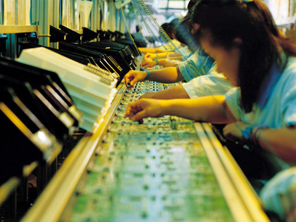
Next the larger through-hole components are fitted, often on a manual production line. Included are the processor socket, the memory and expansion card slots and the various connectors such as keyboard, mouse, audio and video sockets. The components are fitted to the top side of the board with their pins protruding through pads on the bottom side of the board.

The board then enters a wave soldering machine. This contains a tank of molten solder that's pumped across a submerged edge, causing a raised wave of solder. As the board progresses through this apparatus, each part of the bottom side of the board comes into contact with the solder wave. The solder adheres to the board wherever it's free of solder resist, thereby making mechanical and electrical connections between the component leads and the pads.
10. Final testing and packaging
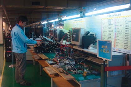
For final testing, processor and memory modules are plugged into their sockets. External PC components such as a hard disk, CD/DVD drive, monitor, keyboard and so on are also plugged into their appropriate connectors. With the motherboard now effectively built into a complete PC, a full functional test involving every socket is carried out.

This is mostly an automated process, although humans do still have a part in the process for areas like audio circuitry. All this is followed up with a 'burn-in' test, which involves running diagnostic software on the motherboard for a protracted time while it's subjected to high temperatures and temperature cycles.
If the board passes this test, which is designed to cause any potentially faulty components to fail, the motherboard is complete. All that remains is for the finished board to be packaged in an antistatic bag and box, and it's ready to take pride of place in a new PC.
- 1
- 2
Current page: 6-10: Assembling the motherboard
Prev Page 1-5: What goes into making a motherboard?