Google's Tensor Processing Unit explained: this is what the future of computing looks like
Specialized silicon will lead the way forward
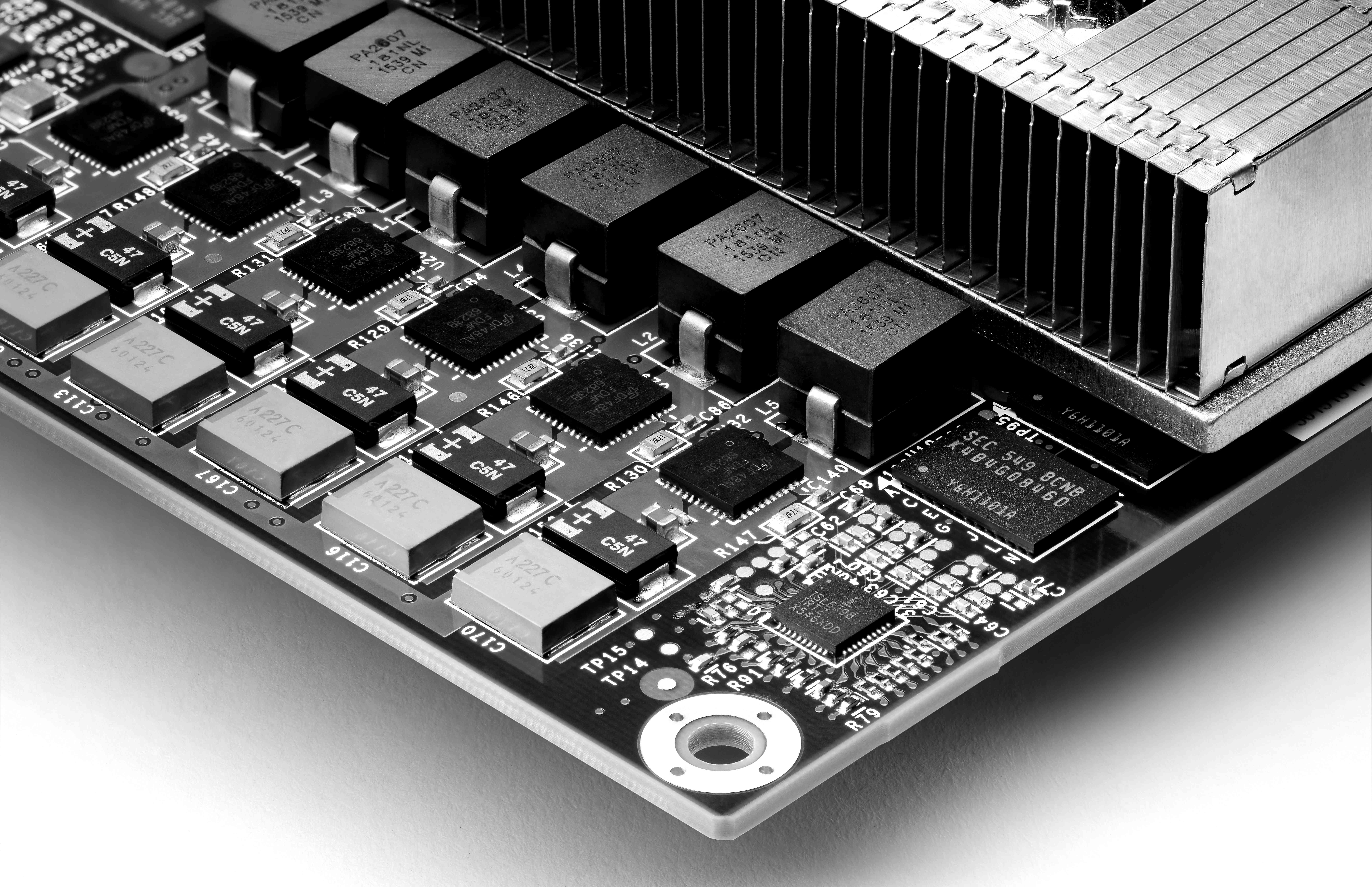
When Google unveiled its Tensor Processing Unit (TPU) during this year's Google I/O conference in Mountain View, California, it finally ticked for this editor in particular that machine learning is the future of computing hardware.
Of course, the TPU is only a part of the firm's mission to push machine learning – the practice that powers chat bots, Siri and the like – forward. (It's also the chip that defeated the world Go champion recently.) Google also has TensorFlow, its open source library of machine intelligence software.
And sure, the chips that we find in our laptops and smartphones will continue to get faster and more versatile. But, it seems as if we've already seen the extent of the computing experiences that these processors can provide, if only limited by the devices they power.
Now, it's the TPU, a meticulous amalgamation of silicon built specifically for one purpose, and other specialized processors both already here (like Apple's M9 co-processor) and to come, that stands to push the advancement of mankind's processing power – and in turn our device's capabilities – further and faster than ever before.
So, we wanted to learn more about this new kind of chip, how it's different exactly, just how powerful it is and how it was made. While Google Distinguished Hardware Engineer Norm Jouppi wouldn't disclose much about the chip's construction (it's apparently just that special to Google), he enlightened us over email regarding just what the TPU is capable of and its potential for the future of machine learning.
TechRadar: What is the chip exactly?
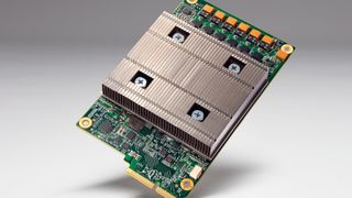
Norm Jouppi: [The] Tensor Processing Unit (TPU) is our first custom accelerator ASIC [application-specific integrated circuit] for machine learning [ML], and it fits in the same footprint as a hard drive. It is customized to give high performance and power efficiency when running TensorFlow.
Get daily insight, inspiration and deals in your inbox
Sign up for breaking news, reviews, opinion, top tech deals, and more.
Great software shines even brighter with great hardware underneath it.
What makes the TPU different from your standard processor specifically?
TPUs are customized for machine learning applications using TensorFlow. Note that we continue to use CPUs [central processing units] and GPUs [graphics processing units] for ML.
How does the chip operate any differently from normal CPUs?
Our custom TPU is unique in that it uses fewer computational bits. It only fires up the bits that you need, when you need them. This allows more operations per second, with the same amount of silicon.
What makes this approach to computational processing better than standard processors at machine learning specifically?
Great software shines even brighter with great hardware underneath it. By building custom hardware for machine learning, we're able to tackle new research and increase our potential to do so much more with ML-powered applications. By custom building the ASIC, we are able to deliver an order of magnitude better-optimized performance per watt for machine learning, and it's tailored for TensorFlow.
Using Google's fleet of TPUs, we can find all the text in the Street View database in less than five days.
How powerful is the TPU in relation to standard processors?
TPU offers an order of magnitude better performance per watt than standard solutions you can buy today (more energy efficient).
Is there a relatable figure you can apply to its performance, i.e. what it would be equivalent to?
We're not disclosing specifics, but here are some examples. We've increasingly been integrating our ML to understand the world and improve the accuracy and quality of our maps, and navigation.
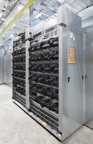
Using Google's fleet of TPUs, we can find all the text in the Street View database in less than five days. In Google Photos, each TPU can process [more than] 100 million photos a day.
If the claim is that the TPU launches Moore's Law forward by three generations, what does that mean for the rest of us?
It's not that we've moved Moore's Law forward by 3 generations, but that the benefits of a specialized ASIC are roughly equivalent to a general-purpose processor using a technology that is three generations better. The benefits of specialization are well-known in the ASIC industry – for example, see slide 26 of Mark Horowitz's "Scaling Power and the Future of CMOS."
We're making the benefits of specialization for TensorFlow widely available through Google services.
Can we expect to see the TPU, or something similar or any learnings from it, impact our everyday devices?
TPUs are making our machine-learning powered services more accurate and useful every day. We don't have anything else to announce today, but we're not standing still.
This article is part of TechRadar's Silicon Week. The world inside of our machines is changing more rapidly than ever, so we're looking to explore everything CPUs, GPUs and all other forms of the most precious metal in computing.
Joe Osborne is the Senior Technology Editor at Insider Inc. His role is to leads the technology coverage team for the Business Insider Shopping team, facilitating expert reviews, comprehensive buying guides, snap deals news and more. Previously, Joe was TechRadar's US computing editor, leading reviews of everything from gaming PCs to internal components and accessories. In his spare time, Joe is a renowned Dungeons and Dragons dungeon master – and arguably the nicest man in tech.
Most Popular


