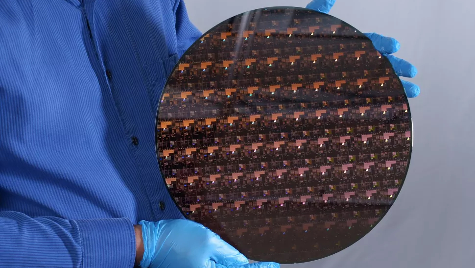
IBM unveils world's first 2nm chip
2nm chips can fit over 300 million transistors in one square millimeter

Computing giant IBM says it has created the first semiconductor with 2 nanometer (nm) nanosheet technology.
IBM projects the major breakthrough will help almost double the performance of the current chips while lower energy use by upto 75% as compared to the widely used 7nm node chips.
The 2nm chips will be able to fit up to 50 billion transistors on a chip the size of a fingernail, reportedly at a density of 333 million transistors per square millimeter (MTr/mm2).
- These are the best business computers currently available
- Here's our list of the best business laptops
- We've put together a list of the best workstations on the market
According to AnandTech that’s considerably higher than TSMC’s 5nm (171.30 MTr/mm2) and Intel’s 7nm (237.18 MTr/mm2).
“It [the 2nm chip] is the product of IBM’s approach of taking on hard tech challenges and a demonstration of how breakthroughs can result from sustained investments and a collaborative R&D ecosystem approach,” said Darío Gil, SVP and Director of IBM Research.
Energy efficient
IBM contends that the 2nm chip will help satiate the demand for increased chip performance and energy efficiency, especially with the onslaught of the hybrid cloud, increase in artificial intelligence workloads, and demand for Internet of Things devices.
IBM puts the energy efficiency of the 2nm chips in perspective by saying that when used inside cell phones they could quadruple the battery life of cell phones that currently use processors based on 7nm, such as the iPhone 11, Samsung Galaxy S10 and Google Pixel 5.
Are you a pro? Subscribe to our newsletter
Sign up to the TechRadar Pro newsletter to get all the top news, opinion, features and guidance your business needs to succeed!
The researchers also note that processors based on the new 2nm technology could dramatically slash the carbon footprint of data centers, and also help reduce the reaction time in autonomous vehicles like self-driving cars by speeding up object detection.
The 2nm technology was developed in IBM’s Albany, NY lab and is slated to go into production towards the end of 2024.
- Need something more portable? Check out the best mobile workstations
With almost two decades of writing and reporting on Linux, Mayank Sharma would like everyone to think he’s TechRadar Pro’s expert on the topic. Of course, he’s just as interested in other computing topics, particularly cybersecurity, cloud, containers, and coding.
