Intel might have a plan to keep up with Moore's Law
Intel patent shows plan for stacking transistors for better performance

Intel is a company in a spot of bother: TSMC, Apple, and other rivals are outpacing its chip technology and Moore's Law – literally created by Intel's founder – is starting to cause the chipmaker some headaches.
However a patent unearthed by Twitter user @Underfox3 has found that the company could well be developing a plan: stacking transistors on top of each other for better performance in less space. Now, of course, this is only a patent – companies patent weird and whacky things all the time for a variety of reasons, most likely to prevent competitors from getting the jump on them.
But there is something interesting about Intel thinking its way around the problem of how to squeeze more power into ever-smaller spaces - namely, if this design comes to fruition, Intel could be looking at sub-2 nanometer (nm) processes.
Patent: Stacked Forksheet Transistors - Intel"The combination of shared-gate stacked nanoribbon transistors with a self-aligned dielectric wall can eventually lead to an ultimately scaled 3D stacked forksheet CMOS architecture. (...)"More details: https://t.co/bJjuD7rlRH pic.twitter.com/ZZvYLNAedWJanuary 13, 2022
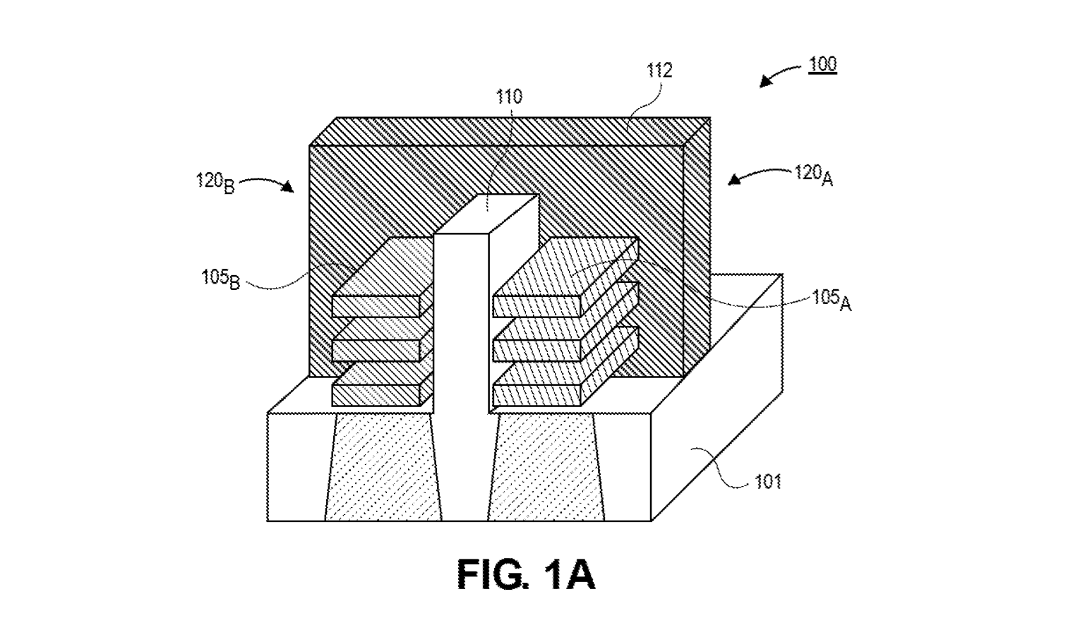
Intel calls the design "stacked forksheet transistors" and you can see why: the transitions would be stacked on top of each other.
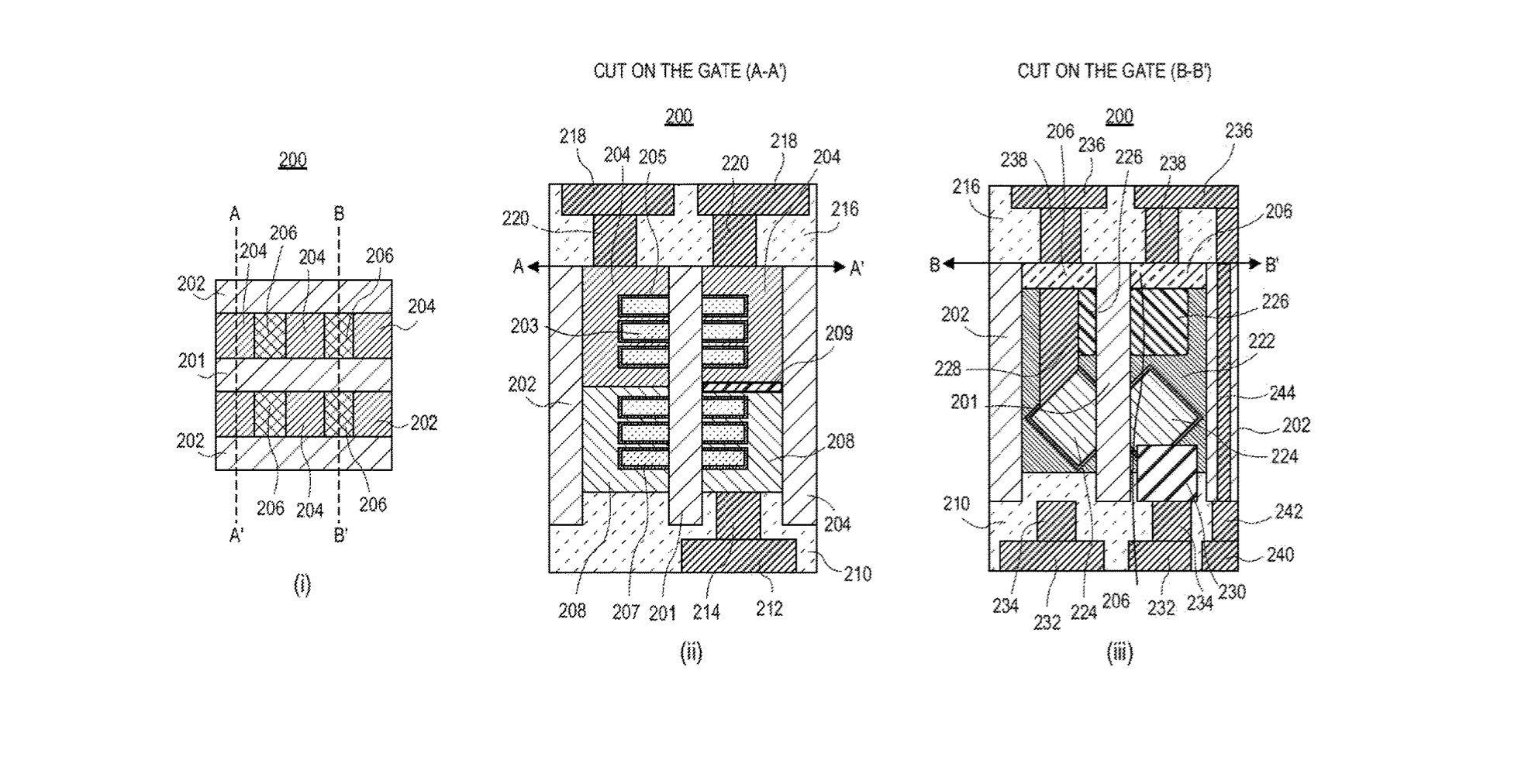
As Intel explains: "A first transistor device includes a first vertical stack of semiconductor channels adjacent to an edge of the backbone. A second transistor device includes a second vertical stack of semiconductor channels adjacent to the edge of the backbone. The second transistor device is stacked on the first transistor device."

The end result from this extremely nerdy patent application is that Intel could create a 3D vertically-stacked CMOS architecture, allowing for increased transistor counts over today's current architectures – a huge boost for the company. The company does note however that, as it stands, the constraints are "overwhelming".
It's impossible to tell exactly what kind of performance uplift could be achieved by Intel's design, and the company conspicuously doesn't speculate, but TSMC moving from a 5nm process to a 3nm process resulted in 10% to 15% performance gains while using up to 30% less power.
Are you a pro? Subscribe to our newsletter
Sign up to the TechRadar Pro newsletter to get all the top news, opinion, features and guidance your business needs to succeed!

Whether this patent ever makes it into production or not, it's interesting to see Intel working through the problem of how to squeeze more power out of less, especially as the company begins its transition under new CEO Pat Gelsinger. A sub-2nm process would be game changing, putting Intel in-line with Apple's incredibly impressive M1 series processors.
- These are the best business laptops around
Via Tom's Hardware
Max Slater-Robins has been writing about technology for nearly a decade at various outlets, covering the rise of the technology giants, trends in enterprise and SaaS companies, and much more besides. Originally from Suffolk, he currently lives in London and likes a good night out and walks in the countryside.