Self-assembling chips could help us keep pace with Moore's law
Bypassing fundamental physical limits

Moore's Law, the observation that the number of transistors in a chip doubles every two years or so, has held for about half a decade.
In the early 2000s it began to falter, as chip manufacturers began to bump up against fundamental physical limits. But ways were found to bypass those limits, and transistor density continued to double roughly every two years.
While Intel has been talking about keeping the law alive in increasingly-difficult circumstances by making bigger improvements less often, a team of engineers at MIT believes that they've found a smart way to make smaller microchip patterns than ever.
Three-stage technique
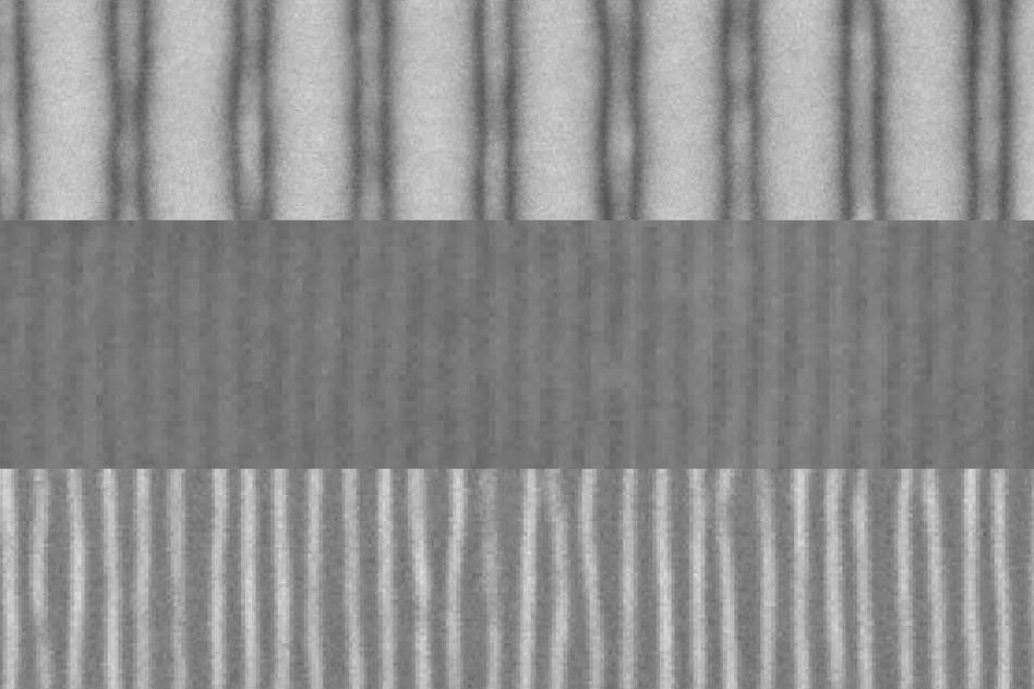
Their approach uses a three-stage technique. First an electron beam is used to write a pattern of lines onto the surface of a chip. Then, a mix of materials known as a "block copolymer" is laid down.
This mix will naturally segregate itself into predictable patterns. By adjusting the size of the block copolymer, different patterns can be created. “One half is friendly with oil, the other half is friendly with water,” explained Do Han Kim, leader author on a paper describing the discovery. “But because they are completely bonded, they’re kind of stuck with each other.”
Finally, a thin, protective polymer film is formed on a surface by heating it up and allowing it to condense, just like water vapour from a hot shower condenses on a cold mirror. This top coating forces the block copolymers to assemble in a certain way, guided by the underlying pattern, and it can be etched on to build another layer over the top.
Cost-effective
While there are other ways to achieve this kind of fine patterning, the team says that none of them are as cost-effective for large-scale manufacturing as this method. Most facilities already perform the etching step, and adding the other steps should be relatively easy.
Get daily insight, inspiration and deals in your inbox
Sign up for breaking news, reviews, opinion, top tech deals, and more.
“You wouldn’t need to change all those machines," said Karen Gleason, MIT's associate provost. "And everything that’s involved are well-known materials.”
“Being able to create sub-10-nanometer features with polymers is major progress in the area of nanofabrication,” said Joerg Lahann, a professor of chemical engineering at the University of Michigan, who was not involved in the work.
“The quality and robustness of this process will open an entirely new area of applications, from nanopatterning to nanotribology.”
The full details of the research were published in Nature Nanotechnology.
