The future of leading-edge chips according to TSMC: 5nm, 4nm, 3nm and beyond
TSMC details process technologies that will be used for billions of chips
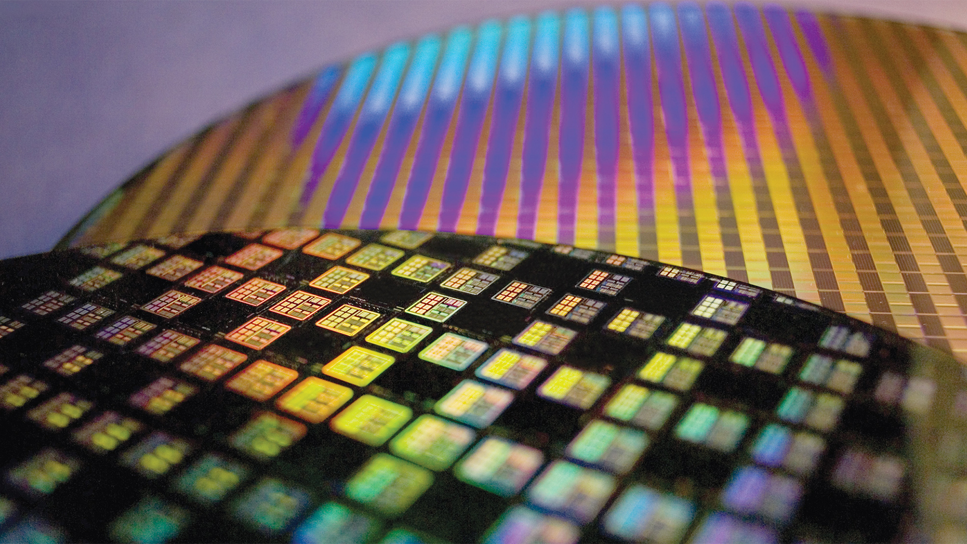
Taiwan Semiconductor Manufacturing Co. (TSMC) recently shared some details about its progress and plans for the coming years.
TSMC will continue to introduce new leading-edge manufacturing processes annually; 5nm chips this year and 3nm processors in late 2022.
For customers that need more than a leading-edge node, meanwhile, TSMC will offer new packaging technologies that will enable to create ultra-compact SiPs, as well as behemoth-sized SoCs for supercomputers.
- We've built a list of the best mobile workstations out there
- There is also our list of the best business computers available
- Looking for something more powerful? Here's the best workstations you can buy
TSMC: a $400 billion company
There are only a few companies in the world with leading-edge process technologies that can be used to build highly-complex processors for datacenters and supercomputers, GPUs, and smartphone SoCs. Intel and Samsung Electronics are integrated device manufacturers (IDMs) that are focused on both chip design and process nodes. By contrast, TSMC is a pureplay foundry that is focused on production and nothing else.
Valued at nearly $400 billion (as of late August, 2020), TSMC is the world’s largest contract maker of semiconductors that produces some of the most advanced chips today, for companies like Apple, AMD, Nvidia, and Intel. To a large degree, TSMC’s process technologies and capabilities define what its clients will be able to offer, so it is important to watch TSMC and its plans closely.
TSMC recently held its annual Technology Symposium where it revealed details about its progress with its current and future leading-edge nodes, as well as many other important factors for the future of chips.
TSMC N5: in production with good yields
TSMC confirmed that it had started high volume production of chips using its N5 (5nm) process technology earlier this year. According to the world’s leading contract maker of semiconductors, the new process has lower defect densities than the previous generation node at the same time of its lifespan, which is a positive news for TSMC clients.
Are you a pro? Subscribe to our newsletter
Sign up to the TechRadar Pro newsletter to get all the top news, opinion, features and guidance your business needs to succeed!
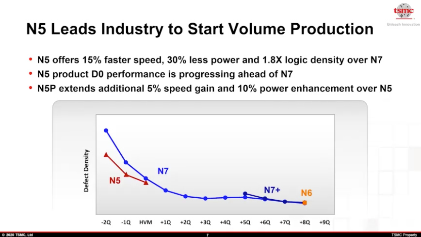
When compared to TSMC’s N7 process technology (which is used to make AMD’s latest Epyc and Ryzen 3000/4000-series CPUs), the company’s N5 node promises to increase performance by up to 15% at the same power, or reduce power consumption by up to 30% at the same clocks and complexity.
Further, transistor density of TSMC’s N5 is up to 1.8x higher than that of N7, but not at all transistor structures. For fabless chip designers, these improvements mean ability to meaningfully boost frequencies of their chips as well as add features due to higher transistor budgets.
TSMC’s 5nm process technology extensively uses extreme ultraviolet (EUV) lithography on 10+ layers to reduce mask count to 81 and avoid usage of multipatterning where possible, which optimizes costs and may improve yields.
TSMC says that its 5nm fabrication process has significantly lower defect density when compared to 7nm early in its lifecycle. This means that current yields of 5nm chips are higher than yields of 7nm chips two years ago. Still, it will take N5 some time to get where N7 is today.
As a rule, TSMC does not disclose which of its customers are using its latest nodes, but AMD has already confirmed plans to use TSMC’s N5 process technology and Apple is also likely to use N5.
TSMC N5P: on track for next year, 10% higher performance
Next year TSMC plans to introduce a performance-enhanced version of the N5 process called N5P, which promises to boost frequencies by up to 5% or reduce power consumption by up to 10%.
TSMC’s N5 and N5P nodes are very similar, so almost any design implemented using the former can be quickly adopted for the latter for performance or power gains. Not all N5 customers are going to use N5P, but some of them might.
TSMC N4: due in 2022, easy to implement
TSMC’s N5 is the so-called long node that is set to be used and evolve for years to come. The next step in N5’s program is called N4, which is expected to enter risk production in Q4 2021 and volume production sometimes in 2022.
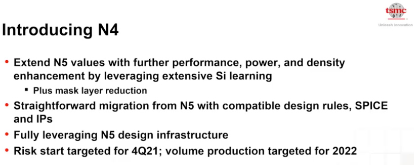
TSMC’s 4nm process technology will extend usage of EUV lithography tools, which will allow the firm to reduce masks count and costs further. The company has not disclosed any information about expected improvements, but N4 expected to be good enough to motivate customers to use the technology.
One of the most important aspects of N4 is that it features N5-compatible design rules, SPICE (simulation program with integrated circuit emphasis) models and IP. To that end, it will be very easy for SoC developers with 5nm designs to adopt TSMC’s 4nm technology and even re-use some of the building blocks they already have.
TSMC N3: significant improvements for upcoming chips
TSMC’s N3 manufacturing technology will be a brand-new node that promises to bring substantial transistor density improvements for high-end processors designed by companies like Apple, AMD, and Nvidia as well as various emerging players working on specialized AI SoCs.
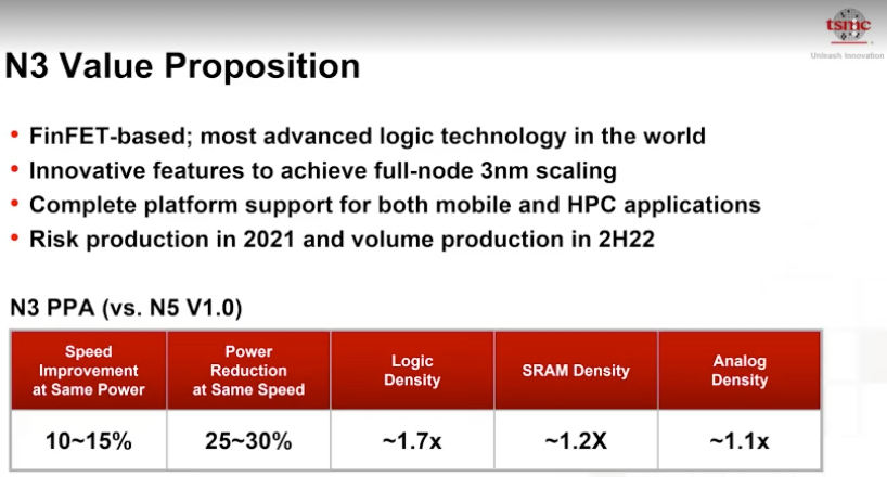
When compared to TSMC’s existing N5 manufacturing process, the new N3 technology promises to increase performance by 10% – 15% (at the same power) or cut power consumption by 25% – 30% (at the same performance), and improve transistor density by up to 1.7 times for some logic structures, up to 1.2 times for SRAM cells, and only up to 1.1 times for analog structures.
It should be noted that not all N3 structures are set to shrink by up to 1.7 times when compared to N5, so actual chip level transistor density improvement may be around 33%. Meanwhile, even a 33% transistor density increase represents a significant advantage for complex chips, such as CPUs, GPUs, and mobile SoCs.
The new node will use both deep-ultraviolet (DUV) and extreme-ultraviolet (EUV) lithography, but it is reasonable to expect usage of EUV to increase, which is what enables performance/power and transistor density improvements.
TSMC plans to start high-volume production (HVM) of chips using its N3 fabrication technology sometimes in the second half of 2022.
TSMC N3: play it safe with FinFETs
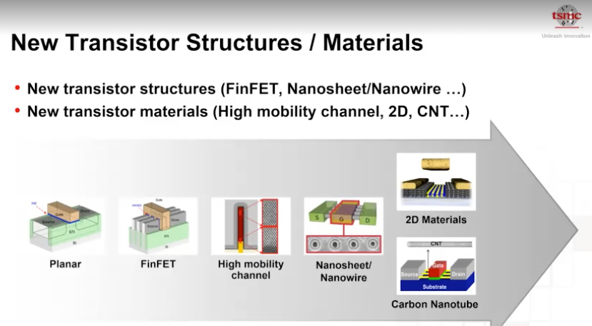
TSMC’s N3 technology will continue to use FinFET technology, the same transistor structure used today. By contrast, Samsung Foundry will switch to gate-all-around (GAAFET) transistor structure with its 3nm process, in a bid to get a substantial generation-to-generation performance and power efficiency gain.

TSMC decided to retain the existing type of transistors for N3 to ensure the technology is rolled out on schedule.
GAAFETs (also known as stacked carbon nanosheets/nanowires) have numerous advantages, but they are harder to produce. Further, usage of new transistor structures requires a whole new stack of electronic design automation (EDA) tools and necessitates development of all-new IP. Ultimately, the switch to GAAFETs may increase design costs, just like switch to FinFETs back in 2014/2015.
So, to play it safe and ensure high initial yields, as well as make life of its customers a bit easier, keeping FinFETs for N3 makes sense. In the end, FinFET structures can be optimized in dozens of ways to extract additional performance, power, and transistor density.
Beyond N3: GAAFETs, new materials
Not using GAAFETs for 3nm does not mean that TSMC does not work on this new transistor structure like other companies do. The contract maker has experimented with GAAFETs for 15 years, so commercial implementation of the technology at a cadence different from a rival is neither good nor bad.
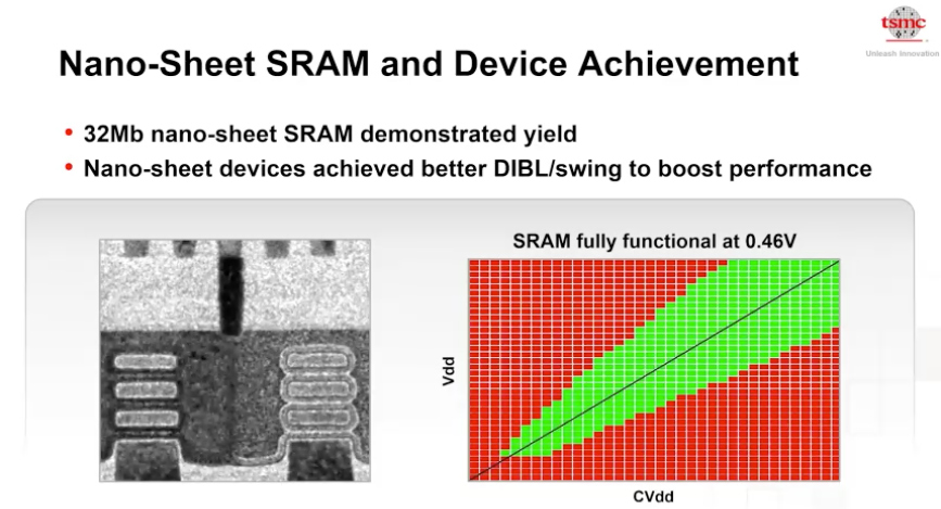
TSMC has demonstrated working 32Mb nanosheet SRAMs at 0.46V with good characteristics. But the company believes that its post-N3 nodes will need more than just a new transistor structure, but will also need new materials that will be good enough for years to come (i.e. TSMC can improve structures without completely changing materials) and improvements to other parts of the chip.
TSMC 3DFabric: enabling skyscraper and behemoth chips
Leading-edge and specialty process technologies allow to build the right silicon using the right methods, but sometimes capabilities of nodes are not enough. This is where TSMC’s comprehensive family of 3D/2.5D silicon stacking and advanced packaging technologies comes in.
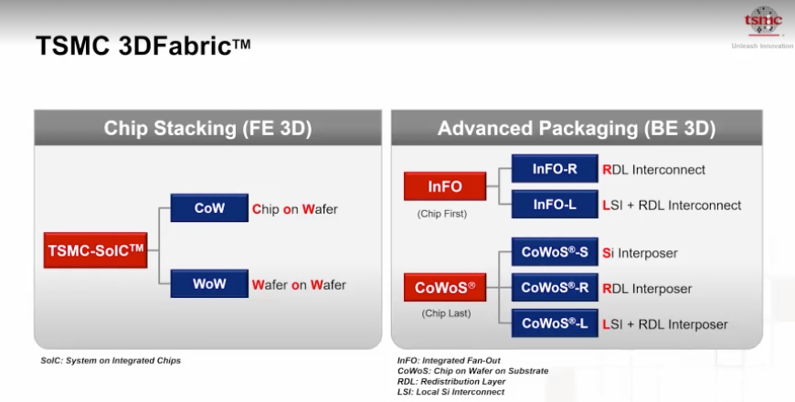
TSMC’s 3DFabric family of technologies includes 2D and 3D frontend and backend interconnect technologies. The frontend subfamily includes such 3D solutions as Chip-on-Wafer (CoW) and Wafer-on-Wafer (WoW) that allow to precisely stack similar and dissimilar dies. The backend subfamily includes well-known Chip-on-Wafer-on-Substrate (CoWoS) and InFO packaging technologies.
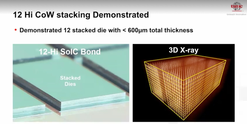
At its Technology Symposium, TSMC demonstrated how it can build a 12-Hi CoW design with a 600µm thickness using through silicon vias (TSVs). This ‘skyscraper’ technology enables to stack up to 12 chips together to get extra performance with additional compute dies, add HBM memory or NAND storage, or improve power delivery with deep trench capacitors, all on a very small footprint. Such advanced system-in-packages (SiPs) might enable applications not possible today.
The AI megatrend drives demand for chip performance at a rather rapid pace, but at the same time, transistor shrinks are slowing down. To that end, there is a growing interest in building large chips in general - and chips larger than the reticle size of a lithography machine in particular.
For example, the reticle size of today’s DUV and EUV scanners is 26 mm by 33 mm, or 858 mm². This defines the maximum size of a chip, or a chip with HBM2E memory on an interposer. To make something larger, chip-sticking (or rather interposer-sticking, to be more precise) technologies like CoWoS are needed.
Last year, TSMC built a 1,700mm² solution for Broadcom using two 5nm dies. At the Technology Symposium, TSMC showcased its CoWoS roadmap that shows 3X reticle-sized CoWoS-enabled assemblies in 2021, as well as a 4X reticle-size CoWoS assemblies in 2023.
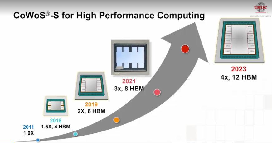
The behemoth-sized 4X reticle chip assembly will feature a whopping size of around 3,400mm² - the size of a small chocolate bar.
Considering architectural and node-related improvements expected by 2023, it is fair to expect such behemoth multi-die chips to offer 6X – 7X peak theoretical performance of today’s flagship solutions. How about GPUs with a whopping 126 FP32 TFLOPS compute horsepower (A100 x6.5) three or four years from now?
To enable such massive theoretical performance, each 4X chip assembly will be equipped with 12 HBM2 memory stacks, which means a 12,228-bit bus. Even using currently available SK Hynix’s HBM2E 3600MT/s memory chips, that translates into an incredible 5.53TB/s memory bandwidth.
Summary
Having landed orders from the world’s leading chip designers, TSMC must introduce new process technologies every year to enable improvements of its clients’ processors on an annual cadence. This is exactly what TSMC promises with its leading-edge technologies in the next three or four years.
For those who need to build specialized highly-integrated solutions, TSMC continues to advance its 3DFabric family of packaging technologies.
Anton Shilov is the News Editor at AnandTech, Inc. For more than four years, he has been writing for magazines and websites such as AnandTech, TechRadar, Tom's Guide, Kit Guru, EE Times, Tech & Learning, EE Times Asia, Design & Reuse.