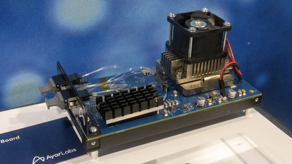
Nvidia-backed startup uses Intel chip to replace electrical signals with light to reach Tbps speeds – here is what it looks like in the flesh
Optical system could be foundational to technologies like 6G, company claims

Ayar Labs has demonstrated an innovative technology that plugs directly into chip packages and uses light to transmit data – reaching blistering transfer speeds.
The firm paired its TeraPHY optical I/O chiplet with a SuperNova multi-wavelength light source, and they bundled this with an Intel Pluggable transceiver module, according to Serve the Home.
On show at SC23 last month, Ayar Labs' TeraPHY chiplet can reach 4Tbps bidirectional bandwidth while only consuming 10W power – which is far greater than lightning speeds of today's high bandwidth memory (HBM) units. For example, Macron's HBM3E units can reach up to 10Gbps of data processing speeds – which pales in comparison to the possibilities using the optical technology that could replace electronic signals – if brought to the market.
Look toward the light
Ayar Labs first teased this technology in March, demonstrating its 4Tbps light-enabled capabilities at the Optical Fiber Communication Conference (OFC).
The technology, in particular, may allow compute, emmory and network silicon to communicate by using only a fraction of the power used today. It also boosts the performance, latency and reach when compared with the performance of electric signals.
Silicon photonics has been discussed in the industry for a while, with Nvidia signing a research and development partnership with Ayar Labs last year to build on the early promise of the technology.
The manufacturer of some of the best GPUs on the market also took part in Series C fundraising, investing into the firm as part of a $130 million package to develop out of band lasers and silicon photonics interconnects.
Are you a pro? Subscribe to our newsletter
Sign up to the TechRadar Pro newsletter to get all the top news, opinion, features and guidance your business needs to succeed!
By plugging the technology directly into chip packages, it could be freed from printed circuit boards and long electrical traces, according to Serve the Home. The module's pluggable form factor also means it can be replaced if things go awry.
If delivered in such a form, Ayar Labs believes it can become foundational to next-generation AI applications, data centers, and dense 6G communications, as well as other applications.
More from TechRadar Pro
- Check out the fastest SSDs out there
- The world’s fastest SSD has just been tested and it packs an unbelievable smart cooling system
- These are the best M.2 SSDs around right now

Keumars Afifi-Sabet is the Technology Editor for Live Science. He has written for a variety of publications including ITPro, The Week Digital and ComputerActive. He has worked as a technology journalist for more than five years, having previously held the role of features editor with ITPro. In his previous role, he oversaw the commissioning and publishing of long form in areas including AI, cyber security, cloud computing and digital transformation.