TechRadar Verdict
It's almost GTX 680 performance for £100 less, but at £300 it still prices itself out of most pockets.
Pros
- +
Great performance
- +
GPU boost
- +
On par with AMD's best
Cons
- -
Rather pricey for a second tier card
Why you can trust TechRadar
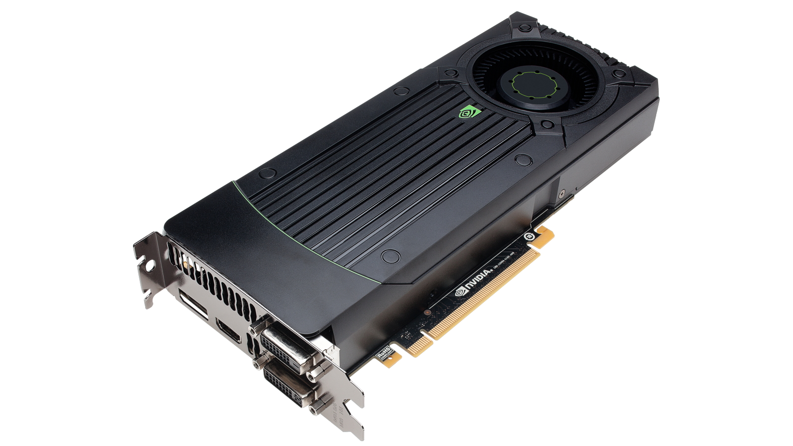
The Nvidia GeForce GTX 670 is here to make a real name for the Kepler architecture in the more mainstream segment of the graphics card market.
Since we saw the first Kepler card, the Nvidia GeForce GTX 680, in cool, crisp sunny San Francisco, we've been itching to get our mitts on the more sensibly priced versions of the new architecture.
The GTX 680 is still sitting over the £400/$500 mark a few months after release and, given the Nvidia GTX 580 didn't have to drop its price throughout its lifespan, we doubt it will change much.
Since then we've seen the Nvidia GeForce GTX 690 tip up, the graphics equivalent of the race spec sports car, all injection-moulded magnesium and multiple GPUs.
But at £830/$1,000 that exceptional card is beyond the financial realms of the typical PC gamer.
So a cut-down version of the GTX 680 is what we've been after, and what we've known was coming, since Kepler first fired up in our test bench. With the Nvidia GeForce GTX 670 that's exactly what we've found ourselves facing.
At its heart is the same GPU that powered the first Kepler card, and as Nvidia puts it, the Nvidia GeForce GTX 670 is "built from the DNA of the GTX 680".
But we're still not calling this the real mainstream Kepler card, that will come in the shape of the GTX 660 that is yet to come. This GTX 670 is aiming squarely at the market currently inhabited by the AMD Radeon HD 7950, so we're talking about a £330/$400 graphics card here.
The GTX 660 though is likely to come with a new GPU spin, not just the slightly chopped down GK104 GPU that sits at the heart of the Nvidia GTX 670 and its redesigned PCB.
So then, what sits on that redesigned circuit board?
Vital stats
GPU
- GK104
SMX modules
- 7
CUDA cores
- 1,344
Base clock
- 915MHz
Boost clock
- 980MHz
Memory
- 2GB GDDR5
Architecture
When Nvidia says it is using the same DNA as the Nvidia GTX 680 for the GTX 670 it's not just trying to hang on the coat-tails of the current top-end single-GPU card.
The GTX 670 is running the exact same GK104 GPU as the GTX 680, but with one of the new SMX modules chopped out. That means it is running with 7 SMX modules making a total of 1,344 CUDA cores running around inside it.
One of the key differences between the Kepler and Fermi graphics architectures is the now unified shader and GPU clock. In previous generations Nvidia had been running the shader clock at twice the speed of the GPU itself.

That meant that for the relatively limited number of CUDA cores it was cramming into its Streaming Microprocessors (SM) it could squeeze out as much performance as possible. With only 32 CUDA cores per SM that made sense.
With the change in production process to 28nm transistors in Kepler the core count per redesigned SMX has risen dramatically to 192.
From the Nvidia GTX 570 to this GTX 670 then that's a massive 180% increase in CUDA cores.
It's this exponential rise in core count that eases any speed issues that would have otherwise arose in making the CUDA cores run at half the speed they were in Fermi.
Other than the clockspeed, and the sheer number of them though, the CUDA cores in Kepler are identical to the ones that we've had in Fermi for years.
As well as the new SMX modules then, what else does Kepler do differently?
Well, the real big news is down to the Intel Turbo Boost-aping GPU Boost. Nvidia has been very open about the fact it is standing on the CPU company's shoulders on this one.
But take nothing away from Nvidia, making the GPU clockspeed dynamic on a per second basis is thoroughly impressive and enables the card to take advantage of the massive amount of overclocking headroom most GPUs have been born with in the last few generations.
While the clockspeed is a way short of the 1GHz mark the Nvidia GTX 680 was sporting, in the games across our benchmarking suite the Nvidia GTX 670 happily ran at over 1,058MHz.
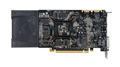
Nvidia has also redesigned the PCB layout too – and is allowing card manufacturers to create their own designs from the get go too.
That should mean we ought to see some interesting designs from the add-in board (AIB) manufacturers at launch, with overclocked cards here, like the Zotac GTX 670 AMP! edition.
The big change has been to move the power circuitry to the 'west' side of the chip. That pushes it close to the bracket side of the board and has created a great deal of space at the end of the card.
This reference design card has taken up this space with the same GPU cooler as chills the heart of the GTX 680, but the PCB itself stops short of the fan.
You can expect to see some small form factor designs, with different coolers, coming our way soon.
