Why you can trust TechRadar
High above the clean, sun-baked streets of San Francisco, in a hotel bar - which bears more than a passing resemblance to the Emperor's throne-room on the unfinished DeathStar – TR finds itself talking to a VP at Nvidia who shall remain nameless.
When challenged that Kepler was essentially just a die-shrink of the Fermi architecture his reaction was not one we expected.
The amount of alcohol imbibed may have had something to do with the vehemence with which he countered the argument, suffice to say he referred to the previous generation in less than glowing terms.
Terms which probably shouldn't find their way into a site so innocent or polite as TechRadar.
He's right though; while there are definite similarities to the last Nvidia graphics technology Kepler is still a different beast to Fermi, and is much more than just the actual hardware too.
But lets cover that die-shrink first.

Like AMD, Nvidia has taken the plunge and gone for a 28nm production process on this generation of its graphics cards. That means compared with the GTX 580 this new GTX 680 can manage a far smaller die size and still cram in more transistors than it ever has before.
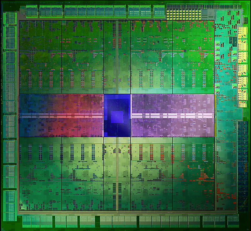
We're talking about the GTX 680's GK104 GPU as a 295mm2 chip compared with the 520mm2 GF110 in the GTX 580.
That's a smaller chip than the GTX 560 Ti with 500 million transistors more than the GTX 580.
It's also a far smaller chip than AMD's 28nm Tahiti GPU at 352mm2, though AMD is claiming almost an extra billion transistors in its top-end chip.
From those simple figures you could infer that the Nvidia architecture is a lot less power-hungry than either its predecessor or the competition, and you'd be right.
The GTX 680 is actually a sub-200w part, operating at its base clock of 1,006MHz at 195w under full load, while the GTX 580 and HD 7970 are 244w and 230w respectively.
So many shaders...
All impressive numbers on the surface but what's actually going on inside, and why are we now talking about a GPU's base clock like it was a CPU?
Despite the ever-bombastic Randy Pitchford of Gearbox referring to it as 'a simulation CPU', because of the advanced PhysX and Apex effects, this is still very much a gamer's GPU.
But Nvidia has taken more than a leaf out of Intel's book; more of that later.
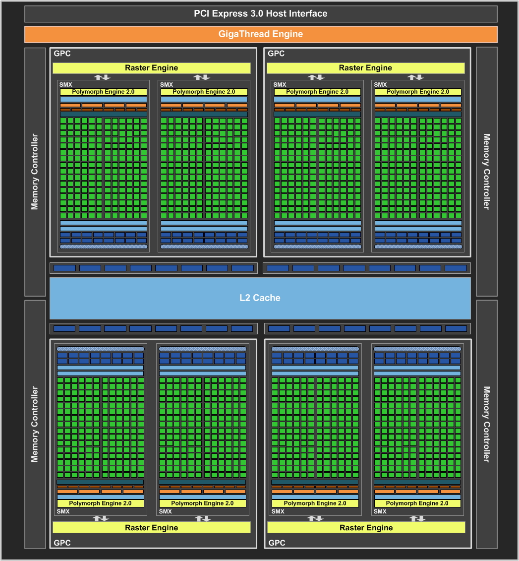
First let's take a look at the actual make up of the GK104 GPU. Like Fermi, the Kepler GPU is made up of multiple CUDA cores jammed into multiple streaming microprocessors (SMs).

These SMs act like simple processors, each concurrently taking on an action, making for impressive parallelism; a cornerstone of GPGPU computing.
But these are no longer called plain ol' SMs, oh no, they are now called SMX, which by today's typical nomenclature probably stands for Streaming Microprocessor Xtreme…
But compared with the old SMs of the Fermi days they could easily be deemed eXtreme. Previously each contained a total of 32 CUDA cores, in Kepler that figure stands at a whopping 192.
Even with half the SM blocks of the GTX 580 you're still looking at 1,536 CUDA cores/shaders spread out over 8 SMXs.
Nvidia is claiming a 2x improvement in terms of performance/watt compared with the GTX 580. That figure seems a little conservative considering the GTX 680 comes with three times the CUDA cores, but while they are physically identical to the cores in the Fermi architecture they are clocked much slower.
In fact they are half as fast because Nvidia has opted not to have a separate shader clock (historically set twice as fast as the GPU clock) instead we have one solitary base clock covering everything.
Boostin' makes us feel good
And there it is again, that base clock.
For every Kepler-based graphics card we are now going to be quoted two separate frequencies, one is the base clock and the second is the Boost clock.
Nvidia has been totally honest and admitted that it copied the idea from Intel, that it is "standing on the shoulders of a great company", as Drew Henry, General Manager of Desktop GeForce puts it.
So we have Turbo Boost for GPUs, the snappily-titled GPU Boost. Asus may have already tried to coin the term on its motherboards, but we doubt there'll be much of a fight over the name.
In previous GPU generations the final clockspeed was determined by the worst-case scenario of application power usage – typically taking the most power hungry app around and setting the clockspeed to match that power draw.
But the draw on the GPU varies massively between different programs, just taking Fermi as an example, power for apps could vary by as much as 50%.
So on lower powered apps there's a lot of GPU headroom not being utilised.

GPU Boost then analyses the amount of power an application is using and boosts the GPU frequency with the amount of extra headroom it then has at its disposal.
It's also completely application independent – you wont need a new Kepler profile when a game gets released so that GPU Boost can take advantage.
It's all based on measurements coming directly from the GPU's sensors in real-time.
Kepler can dynamically alter its clock and voltage every 100ms, essentially every few frames the GPU has a decision to make on clocks and voltage settings.
And as this is just the first generation of GPU Boost you can expect that to be done quicker over time.
This auto-overclocking though doesn't mean an end for traditional overclocking.
"GPU Boost is like overclocking's little buddy… our GTX 680 is a monster overclocker," says Tom Petersen, Nvidia's director of technical marketing.
Each of Nvidia's partner card manufacturers has been given all the API goodness with which to prepare their own overclocking apps, though we had a look at EVGA's Precision tool.
There are two sliders, one for altering the base clock and one for allowing the GPU to use extra power – up to just over 260w. And GPU Boost will still work when you've slammed both those sliders to max too.
Just as interesting is the Frame Rate Target.
You can set the software to target a particular frame rate – this is really only used to set a target, not to force the GPU to overclock to get there.
But if you give the GPU the frequency headroom and the capability to draw as much power as it can then it will push the clocks up to ensure it hits your specific frame rate.
This is arguably more interesting at the mid-range than the high-end. The prospect of being able to tell your £200 card to hit 30FPS in all games will give even the least savvy PC gamer console-like performance with minimal effort.
It's a tantalising prospect and shows that Nvidia is really focusing this release on the gamer, not the GPU compute all-rounder that Fermi had been touted as.
