Why you can trust TechRadar
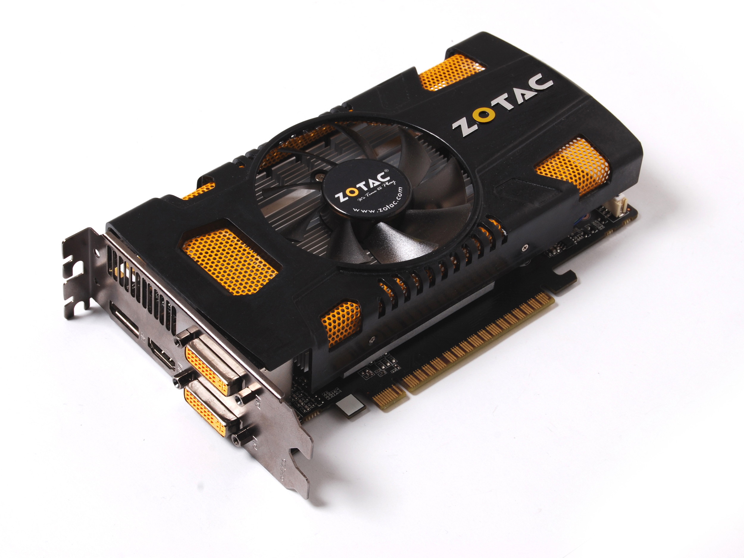
Based on yet another spin of the Fermi core, the GeForce GTX 550 Ti uses the new GF116 core.
This core has a lot in common with the GPU it's destined to replace, the GF106 found in the GTS 450.
Created using a 40nm fabrication process, and measuring a mere 238mm2, this is a core made for a pricepoint more than for setting the polygon-pushing world alight.
Inside the relatively small die, you'll find 1,170 transistors strutting their stuff, offering up 192 CUDA cores. Indeed, the first impressions will show that there's very little on offer in the GTX 550 that wasn't available previously in the GTS 450.
There are some notable exceptions though.
Where the GTS 450 boasts 16 Render Output units (ROPs), the GTX 550 Ti has 24. This, combined with the notably wider 192-bit memory bus, as opposed to the GTS 450's 128-bit bus, should mean that this new chip outperforms its predecessor significantly when it comes to heavy post-processing titles.
The big news for the GeForce GTX 550 Ti though is that the new GF116 core has been streamlined, so that it can operate at much higher frequencies than its predecessor could manage.
This means that the base GeForce GT 550 Ti is rated to run at 900MHz, and there's room for overclocking as well. This version provided by Zotac has the AMP! suffix, which means that it's overclocked straight out of the box – the core is running at 1,000MHz, equating to a 2,000MHz shader clock.
This is a cool running chip too – in testing the core temperature peaked at 81oC under full load, but importantly, the fan noise was never notable over the background hum of the rest of the system.
Given the requirement for a single 6-pin power connector, and the low 110w TDP, this is a relatively efficient offering from Nvidia.
Current page: Zotac GeForce GTX 550 Ti AMP!: Architecture
Prev Page Zotac GeForce GTX 550 Ti AMP!: Overview Next Page Zotac GeForce GTX 550 Ti AMP!: Benchmarks




Diamond set to become mainstream coolant for AI GPU servers as world’s best thermal conductor promises 25% better overclocking, and 'double performance per watt'

Disappointed by The Electric State? Here's 4 reasons you should watch Tales From the Loop on Prime Video

This impressive 4K drawing display I reviewed was so natural to draw on, I may never use paper again
