TechRadar Verdict
The fastest mainstream SSD around, just not necessarily one to shake the solid state world.
Pros
- +
Speedy performance
- +
Good-value
- +
Five-year warranty
Cons
- -
Not a huge generational leap
- -
Definitely consumer-class SSD
Why you can trust TechRadar
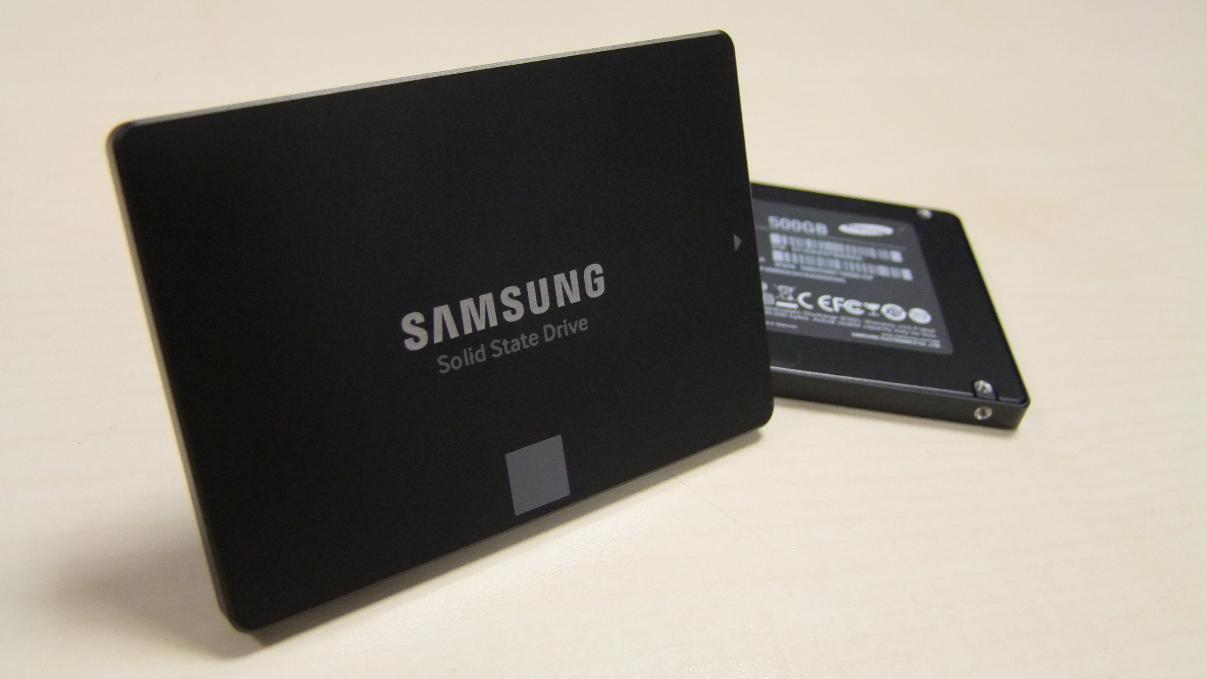
The Samsung 850 EVO is the latest in its affordable line of performance SSDs and shows Samsung's desire to push the solid state game along, even at the lower end of the price/performance stack.
When it comes to solid state drives Samsung has really nailed its colours to the mast; it's going to be first to market with new technologies, it's going to aggressively drive pricing down and it's going to do it all alone.
To that end, the Samsung 850 Pro was the first consumer SSD to show up with 3D stacked memory making up its various components. The Samsung 850 Evo does this as well, using a new spin of the V-NAND tech for its more affordable range of SSDs. And, when we say affordable, we mean it – it’s one of the most value-minded SSDs on the market today.
This new line of SSDs uses a new generation of 3D V-NAND that revolves around piling chips on top of each other, with ‘through silicon vias’ (TSV), which provides connections directly through the stack. This helps boost the bandwidth, as the connections are physically closer, but also means higher capacity drives are more affordable – they can be made without relying on the ever-shrinking of the NAND modules that make up SSDs.
This new generation of 3D V-NAND, then, has been designed to forge a path to higher capacity SSDs in the coming years. Samsung’s second-gen 3D V-NAND is made up of a full 32 layers stacked atop each other in every module. This means, the Samsung 850 Evo has a total density of 86Gbit.
Dense
Now, that's not the highest density NAND you'll find in today's drives - both Crucial and Intel are throwing out drives with 128Gbit density NAND in them and have partnered up to create their own 256Gbit 3D NAND for 2015 - but the difference is Samsung is only using 40nm silicon to get there.
Because of the celebrated shrinking of production processes in all spheres of computing - from processors to memory to graphics chips - it might at first seem like this is a backwards step.
We have, after all, become used to using 19nm NAND in our SSDs, even going as low as 16nm, so using a production process that's more than twice as large would surely undo all the performance and efficiency boosts we picked up along the way down.
But because of 3D V-NAND's ability to hit these high densities with such chunky lithography, combined with the bandwidth boosts of the TSVs inside the stacked modules, the larger dies don't have any impact on relative performance.
The efficiency gains from previous production shrinks are also largely offset by the power reductions in the switch from 2D to 3D NAND.
Samsung estimates a 30% reduction in operational power with the Samsung 850 EVO compared with the older Samsung 840 EVO.
Hardy NAND
The 40nm process comes into its own though when we start talking about endurance.
The biggest benefit is the fact the larger production processes are more reliable and longer-lived than their smaller descendants. When you're making the switch, as Samsung is, from the 2-bit multi-layer cell (MLC) design of its higher-end 850 Pro to the less-robust 3-bit MLC, any endurance boost is welcome.
Traditionally 3-bit MLC doesn't last so long as the 2-bit kind, which is why you'll see the Samsung 850 Pro rocking a full ten-year warranty.
With the 40nm 3-bit MLC of the Samsung 850 EVO it does have a shorter five-year warranty, but that's still a good deal longer than the rest of the affordable SSD world with their three-year hedged bets.
